- 您现在的位置:买卖IC网 > Sheet目录1996 > ICS180M-51LF (IDT, Integrated Device Technology Inc)IC CLOCK GEN LOW EMI 8-SOIC
ICS180-51
LOW EMI CLOCK GENERATOR
SSCG
IDT / ICS LOW EMI CLOCK GENERATOR
2
ICS180-51
REV C 051310
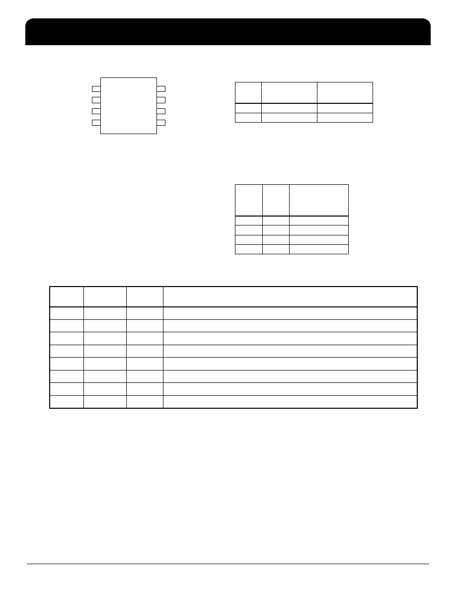
Pin Assignment
Spread Spectrum Select Table
0 = connect to GND
1 = connect directly to VDD
Note: SS% pin has an internal pull-up resistor
Frequency Range Selection Table
Pin Descriptions
1
2
3
X1/CLKIN
4
X2
GND
FS1
SS%
VDD
CLKOUT
8
7
6
5
FS2
8 pin (150 mil) SOIC
SS%
(Pin 4)
Spread
Direction
Spread
Percentage (%)
0
Center
+/-0.625%
1
Center
+/1.875%
FS2
(Pin 8)
FS1
(Pin 7)
Frequency
Range Selection
(MHz)
00
8-10
0
1
10-15
1
0
15-18
1
18-28
Pin
Number
Pin
Name
Pin Type
Pin Description
1
X1/CLKIN
Input
Crystal or Clock Input.
2
X2
Output
Crystal output. Float for a clock input.
3
GND
Power
Connect to ground.
4
SS%
Input
Select pin for spread amount. See table above. Internal pull-up resistor.
5
CLKOUT
Output
Spread spectrum clock output per table above.
6
VDD
Power
Connect to 3.3 V or 5 V.
7
FS1
Input
Select pin for input frequency. See table above. Internal pull-up resistor.
8
FS2
Input
Select pin for input frequency. See table above. Internal pull-up resistor.
发布紧急采购,3分钟左右您将得到回复。
相关PDF资料
ICS180M-52LF
IC CLOCK GEN LOW EMI 8-SOIC
ICS180M-53LF
IC CLOCK GEN LOW EMI 8-SOIC
ICS181M-53T
IC CLOCK GEN LOW EMI 8-SOIC
ICS181MI-01LF
IC CLOCK GEN LOW EMI 8-SOIC
ICS2402MLFT
IC MULTIPLIER/ZD BUFFER 8-SOIC
ICS270PGILF
VCXO CLK TRPL PLL PROGR 20-TSSOP
ICS281PGILF
IC CLK SYNTH TRPL PLL 16-TSSOP
ICS411MLF
IC PC PERIPHERAL CLOCK 8-SOIC
相关代理商/技术参数
ICS180M-51LFT
功能描述:IC CLOCK GEN LOW EMI 8-SOIC RoHS:是 类别:集成电路 (IC) >> 时钟/计时 - 时钟发生器,PLL,频率合成器 系列:- 标准包装:2,000 系列:- 类型:PLL 时钟发生器 PLL:带旁路 输入:LVCMOS,LVPECL 输出:LVCMOS 电路数:1 比率 - 输入:输出:2:11 差分 - 输入:输出:是/无 频率 - 最大:240MHz 除法器/乘法器:是/无 电源电压:3.135 V ~ 3.465 V 工作温度:0°C ~ 70°C 安装类型:表面贴装 封装/外壳:32-LQFP 供应商设备封装:32-TQFP(7x7) 包装:带卷 (TR)
ICS180M-51T
功能描述:IC CLOCK GEN LOW EMI 8-SOIC RoHS:否 类别:集成电路 (IC) >> 时钟/计时 - 时钟发生器,PLL,频率合成器 系列:- 产品变化通告:Product Discontinuation 04/May/2011 标准包装:96 系列:- 类型:时钟倍频器,零延迟缓冲器 PLL:带旁路 输入:LVTTL 输出:LVTTL 电路数:1 比率 - 输入:输出:1:8 差分 - 输入:输出:无/无 频率 - 最大:133.3MHz 除法器/乘法器:是/无 电源电压:3 V ~ 3.6 V 工作温度:0°C ~ 70°C 安装类型:表面贴装 封装/外壳:16-TSSOP(0.173",4.40mm 宽) 供应商设备封装:16-TSSOP 包装:管件 其它名称:23S08-5HPGG
ICS180M-52
功能描述:IC CLOCK GEN LOW EMI 8-SOIC RoHS:否 类别:集成电路 (IC) >> 时钟/计时 - 时钟发生器,PLL,频率合成器 系列:- 产品变化通告:Product Discontinuation 04/May/2011 标准包装:96 系列:- 类型:时钟倍频器,零延迟缓冲器 PLL:带旁路 输入:LVTTL 输出:LVTTL 电路数:1 比率 - 输入:输出:1:8 差分 - 输入:输出:无/无 频率 - 最大:133.3MHz 除法器/乘法器:是/无 电源电压:3 V ~ 3.6 V 工作温度:0°C ~ 70°C 安装类型:表面贴装 封装/外壳:16-TSSOP(0.173",4.40mm 宽) 供应商设备封装:16-TSSOP 包装:管件 其它名称:23S08-5HPGG
ICS180M-52LF
功能描述:IC CLOCK GEN LOW EMI 8-SOIC RoHS:是 类别:集成电路 (IC) >> 时钟/计时 - 时钟发生器,PLL,频率合成器 系列:- 标准包装:2,000 系列:- 类型:PLL 时钟发生器 PLL:带旁路 输入:LVCMOS,LVPECL 输出:LVCMOS 电路数:1 比率 - 输入:输出:2:11 差分 - 输入:输出:是/无 频率 - 最大:240MHz 除法器/乘法器:是/无 电源电压:3.135 V ~ 3.465 V 工作温度:0°C ~ 70°C 安装类型:表面贴装 封装/外壳:32-LQFP 供应商设备封装:32-TQFP(7x7) 包装:带卷 (TR)
ICS180M-52LFT
功能描述:IC CLOCK GEN LOW EMI 8-SOIC RoHS:是 类别:集成电路 (IC) >> 时钟/计时 - 时钟发生器,PLL,频率合成器 系列:- 标准包装:2,000 系列:- 类型:PLL 时钟发生器 PLL:带旁路 输入:LVCMOS,LVPECL 输出:LVCMOS 电路数:1 比率 - 输入:输出:2:11 差分 - 输入:输出:是/无 频率 - 最大:240MHz 除法器/乘法器:是/无 电源电压:3.135 V ~ 3.465 V 工作温度:0°C ~ 70°C 安装类型:表面贴装 封装/外壳:32-LQFP 供应商设备封装:32-TQFP(7x7) 包装:带卷 (TR)
ICS180M-52T
功能描述:IC CLOCK GEN LOW EMI 8-SOIC RoHS:否 类别:集成电路 (IC) >> 时钟/计时 - 时钟发生器,PLL,频率合成器 系列:- 产品变化通告:Product Discontinuation 04/May/2011 标准包装:96 系列:- 类型:时钟倍频器,零延迟缓冲器 PLL:带旁路 输入:LVTTL 输出:LVTTL 电路数:1 比率 - 输入:输出:1:8 差分 - 输入:输出:无/无 频率 - 最大:133.3MHz 除法器/乘法器:是/无 电源电压:3 V ~ 3.6 V 工作温度:0°C ~ 70°C 安装类型:表面贴装 封装/外壳:16-TSSOP(0.173",4.40mm 宽) 供应商设备封装:16-TSSOP 包装:管件 其它名称:23S08-5HPGG
ICS180M-53
功能描述:IC CLOCK GEN LOW EMI 8-SOIC RoHS:否 类别:集成电路 (IC) >> 时钟/计时 - 时钟发生器,PLL,频率合成器 系列:- 产品变化通告:Product Discontinuation 04/May/2011 标准包装:96 系列:- 类型:时钟倍频器,零延迟缓冲器 PLL:带旁路 输入:LVTTL 输出:LVTTL 电路数:1 比率 - 输入:输出:1:8 差分 - 输入:输出:无/无 频率 - 最大:133.3MHz 除法器/乘法器:是/无 电源电压:3 V ~ 3.6 V 工作温度:0°C ~ 70°C 安装类型:表面贴装 封装/外壳:16-TSSOP(0.173",4.40mm 宽) 供应商设备封装:16-TSSOP 包装:管件 其它名称:23S08-5HPGG
ICS180M-53LF
功能描述:IC CLOCK GEN LOW EMI 8-SOIC RoHS:是 类别:集成电路 (IC) >> 时钟/计时 - 时钟发生器,PLL,频率合成器 系列:- 标准包装:2,000 系列:- 类型:PLL 时钟发生器 PLL:带旁路 输入:LVCMOS,LVPECL 输出:LVCMOS 电路数:1 比率 - 输入:输出:2:11 差分 - 输入:输出:是/无 频率 - 最大:240MHz 除法器/乘法器:是/无 电源电压:3.135 V ~ 3.465 V 工作温度:0°C ~ 70°C 安装类型:表面贴装 封装/外壳:32-LQFP 供应商设备封装:32-TQFP(7x7) 包装:带卷 (TR)